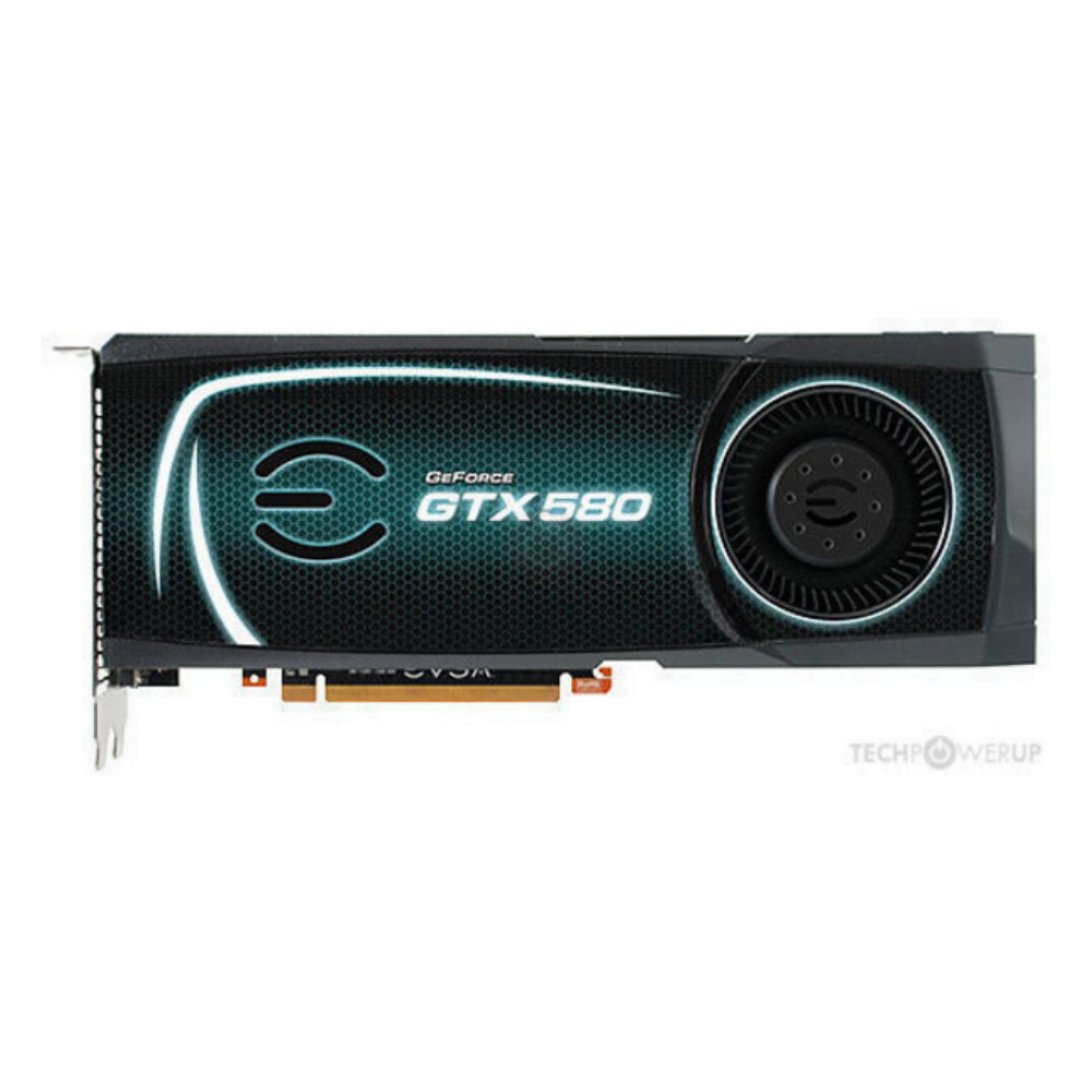
Graphics Processor
- GPU Name
- GF110
- GPU Variant
- GF110-375-A1
- Architecture
- Fermi 2.0
- Foundry
- TSMC
- Process Size
- 40 nm
- Transistors
- 3,000 million
- Die Size
- 520 mm²
Graphics Card
- Release Date
- Nov 9th, 2010
- Generation
- GeForce 500
- Predecessor
- GeForce 400
- Successor
- GeForce 600
- Production
- End-of-life
- Bus Interface
- PCIe 2.0 x16
Clock Speeds
- GPU Clock
- 772 MHz
- Shader Clock
- 1544 MHz
- Memory Clock
- 1002 MHz
4 Gbps effective
Memory
- Memory Size
- 1536 MB
- Memory Type
- GDDR5
- Memory Bus
- 384 bit
- Bandwidth
- 192.4 GB/s
Render Config
- Shading Units
- 512
- TMUs
- 64
- ROPs
- 48
- SM Count
- 16
- L1 Cache
- 64 KB (per SM)
- L2 Cache
- 768 KB
Theoretical Performance
- Pixel Rate
- 24.70 GPixel/s
- Texture Rate
- 49.41 GTexel/s
- FP32 (float) performance
- 1.581 TFLOPS
- FP64 (double) performance
- 197.6 GFLOPS (1:8)
Board Design
- Slot Width
- Dual-slot
- TDP
- 244 W
- Suggested PSU
- 550 W
- Outputs
- 2x DVI
1x mini-HDMI
- Power Connectors
- 1x 6-pin + 1x 8-pin
- Board Number
- P1261 SKU 02
Graphics Features
- DirectX
- 12 (11_0)
- OpenGL
- 4.6
- OpenCL
- 1.1
- Vulkan
- N/A
- CUDA
- 2.0
- Shader Model
- 5.1
GF110 GPU Notes
| GF110 has 4 GPCs each capable of 8 pixels per clock. This limits complete GPU to 32 pixels per clock and because of that it can’t feed all 48 ROPs when they all require data at the same time. Additional ROPs however can be used for MSAA (because it doesn’t require additional data from rasterizers, while giving more work to ROPs.) The complete die contains 64 texture address units and 256 texture filtering units. |

There are no reviews yet.